Compact MBE System Model SVT-V-2
Efficient use of MBE technique for materials research, namely, III-V compound semiconductors.
Features:
- Small Footprint
- 7 Sources
Group III: In, Ga and Al
Group V: As and Bi
Valved cracker for As2
Dopants: for n-type – Si, for p-type Be - Sample Temperature up to 1,000 °C
- Thickness uniformity 1% over 2″ Wafer
- Fast Action Shutters
- Master Wafer Shutter
- Configuration: Load lock and Growth chamber
- Growth module is equipped with the integrated Ion and Titanium sublimation pump system (base vacuum level 5×10⁻⁹ Torr)
- The load lock is equipped with the turbo molecular (base vacuum level 5×10⁻⁸ Torr)
- RoboMBE Process Automation for Growth Recipe Operation
Growth samples:
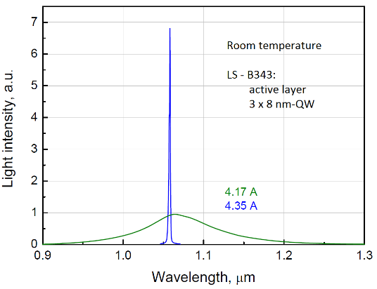
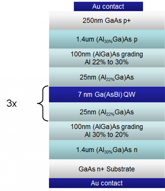
MQW-based Laser structure:
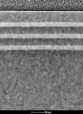
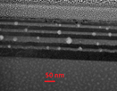
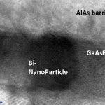
Bi NPs in the GaAsBi QW (HRTEM images):
MBE System Veeco GENxplor R&D
GENxplo MBE system is designed for the epitaxial growth of high quality III-V semiconductor compounds with very high deposition control accuracy on substrates up to 3’’ in diameter for R&D and Small Scale Manufacturing purposes.
Features:
- Extremely high composition and thickness accuracy (error <1.5%);
- 10 Sources
Group III: In, 2xGa and Al
Group V: As, Sb and Bi
Valved cracker for Sb and As2
Dopants: for n-type – Si, Te, for p-type Be - Sample Temperature up to 1,850 °C
- Fast Action Shutters
- Master Wafer Shutter
- Configuration: Load lock and Growth chamber
- Growth module is equipped with the integrated Ion and Titanium sublimation pump system (base vacuum level 5×10⁻⁹ Torr)
- The load lock is equipped with the turbo molecular (base vacuum level 5×10⁻⁸ Torr)